At SPIE Photonics Europe IMS CHIPS contributed as chair and program organizer, sponsor, speaker, and exhibitor.
With two scientific contributions, IMS CHIPS was represented at one of the leading international platforms for photonic technologies. The focus was on two topics that may appear distinct at first glance but are closely linked in their technological depth: diffractive optics for AR/VR/MR systems and multispectral imaging for camera-based pulse measurement.
Both presentations demonstrated how highly precise fabrication enables functional optical systems — and how research on micro- and nanostructures paves the way for applications in communication, medical technology, and immersive systems.
Precise Light Control for Next-Generation Immersive Systems
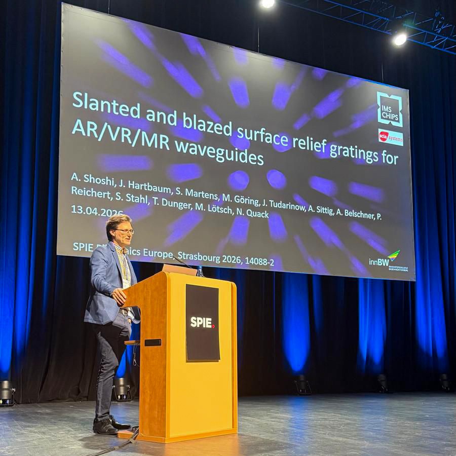
A highlight of the conference program was the presentation by Astrit I. Shoshi and his team. The focus was on a key challenge in modern AR, VR, and MR systems: coupling light into and out of waveguides with high efficiency and precision to enable compact and high-performance systems.
In immersive applications, the quality of optical components is critical. Diffractive structures such as Surface Relief Gratings (SRGs) play a central role as in- and out-coupling elements and contribute to uniform eye-box illumination, which is essential for consistent image quality.
The presentation showed how such complex grating structures can be realized using advanced fabrication strategies based on electron-beam lithography (EBL) and Reactive Ion Beam Trimming (RIBT). The RIBT process enables wafer tilting and controlled material removal through dwell-time modulation, allowing precise adjustment of the grating geometry.
Slanted SRGs are fabricated using a single-level EBL process with a tilted etch, while blazed SRGs use a two-level approach that enables independent control of blaze and anti-blaze angles. Both binary and continuous-height profiles can be realized with high precision in duty cycle, height, and shape fidelity.
What at first sounds like a purely process-related optimization is, in reality, a decisive step toward the future of photonic systems. After all, the more precisely and flexibly such structures can be manufactured, the better optical components can be tailored to specific requirements. The team’s results therefore demonstrate far more than just a successful manufacturing approach: they create a versatile platform for complex diffractive geometries and thus make an important contribution to the further development of highly efficient optics for the next generation of AR/VR/MR applications.
When Diffractive Optics Meet Biomedical Applications
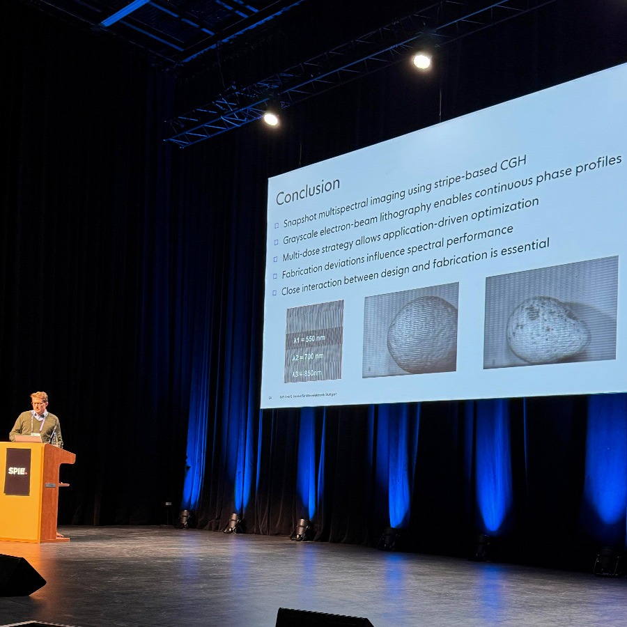
A second contribution by Michael Warber provided insights into a multispectral imaging system for camera-based pulse measurement.
Here, light control is used for a different purpose: instead of guiding light in waveguides, spectral information is encoded within the optical system to enable camera-based pulse detection. The application is based on photoplethysmography, an increasingly relevant method for contactless optical measurement.
The system is based on diffraction at a spatially multiplexed blazed grating structure. To ensure a compact setup, the structure is implemented in reflection.
Fabrication is carried out using grayscale electron-beam lithography followed by aluminum coating. The results show very good agreement between design and fabricated structure. Within the optical system, the diffractive element is positioned in an intermediate image plane, where the local grating structure determines the spectral response.
In the optical system, the diffractive element is positioned in an intermediate image plane. There, the local grating structure determines the system’s spectral response at the corresponding position in the image plane. This not only enables a compact architectural solution but also opens up new avenues for targeted spectral information processing in imaging systems.
This represents a key strength of IMS CHIPS. Research does not end with theoretical design or isolated fabrication but focuses on enabling structures to function in real applications.
Although the presented topics address different application areas, they share a common technological foundation: the ability to design, fabricate, and integrate optical micro- and nanostructures with high precision into functional systems.
This represents a key strength of IMS CHIPS. Research does not end with theoretical design or isolated fabrication but focuses on enabling structures to function in real applications.
The contributions presented at SPIE Photonics Europe 2026 illustrate the interdisciplinary nature of modern photonics research, where materials, processes, design, optical function, and system integration are closely interconnected.
International Visibility for Future-Oriented Research
Participation in SPIE Photonics Europe highlights the international visibility of IMS CHIPS’ work. The conference provides a high-level platform for exchange on current developments in photonics, micro-optics, and system technologies.
The presentation program was complemented by the Marketplace Keynote of institute director Prof. Dr. Niels Quack. In addition to his role as chair, he provided a comprehensive overview of IMS CHIPS activities, including the collaboration with Q.ANT, where photonic AI chips based on thin-film lithium niobate are fabricated.
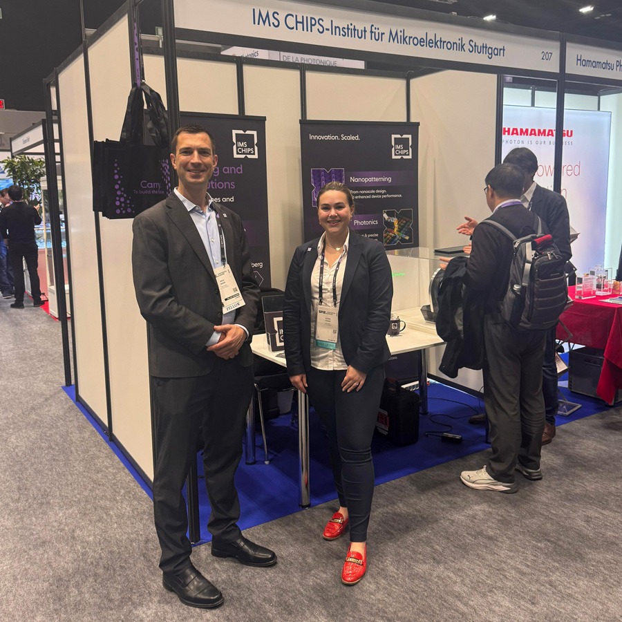
The potential of this material attracted significant interest and was further discussed at the IMS CHIPS booth. The upcoming MPW line for lithium niobate, which will soon be launched at IMS, also received strong attention.
We attracted many of the approximately 2,600 participants to the IMS booth, leading to numerous valuable discussions.
SPIE Photonics Europe 2026 once again demonstrated that the future of photonic systems lies in the precise control of light. The exhibition reflected this breadth, ranging from tool manufacturers and foundries to complete system solutions.
We thank the organizers and look back very positively on the event and the discussions.