
Nanopatterning. For precise structures ranging from the submicrometer to the nanometer scale.
IMS CHIPS develops and manufactures complex micro- and nanostructures tailored to applications in optics, electronics, and life sciences. Our lithography and etching capabilities support binary, multilevel, mesa, and 3D analog structures on resist, quartz, silicon, and SOI wafers as well as mask substrates.
From initial feasibility and process development to qualification and certified small-batch production, we provide the technologies and expertise needed to turn demanding nanopatterning concepts into scalable solutions.
The roadmap from concept to series production.
Get started now.

“Every nanopatterning project starts with a clear understanding of the technical requirements. Together, we define feature size, resolution, materials, substrates, and the appropriate fabrication technology. Based on these parameters, we develop the process flow, assess feasibility, and support your project from initial samples and prototypes through production. If you have a specific application or technical challenge in mind, I’d be happy to discuss it with you.”
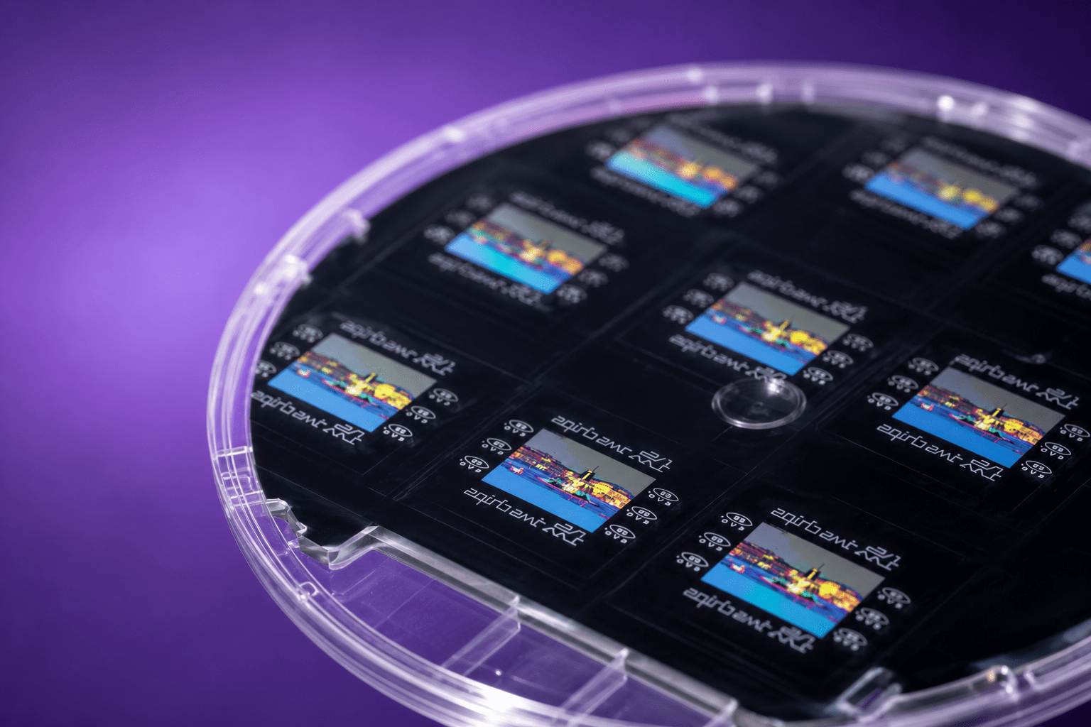
Nanoimprint master. For reproducible nanostructures.
We manufacture replication masters for nanoimprint processes on silicon and quartz wafers, SOI wafers, and mask blanks. Pattern transfer is performed using RIE and ICP processes as well as Bosch and cryogenic etching, allowing the process to be tailored to the substrate and structure requirements.
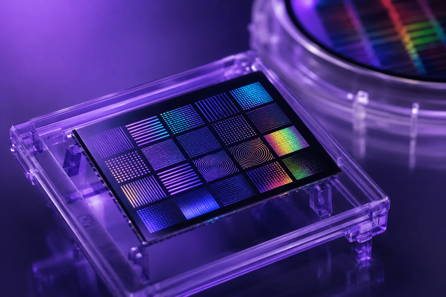
Optical nanostructures. For the precise shaping and control of light.
For optical applications, we precisely pattern fused silica down to the submicron scale. Processing is available on 150 mm and 200 mm quartz wafers as well as 6-inch (6025) and 9-inch (9035) mask substrates. Specialized applications can also be accommodated on 12-inch and 17-inch substrates.
Typical applications include Fresnel lenses, microlens arrays, and diffractive optical elements (DOEs), enabling precise control and shaping of light through micro- and nanostructured surfaces.
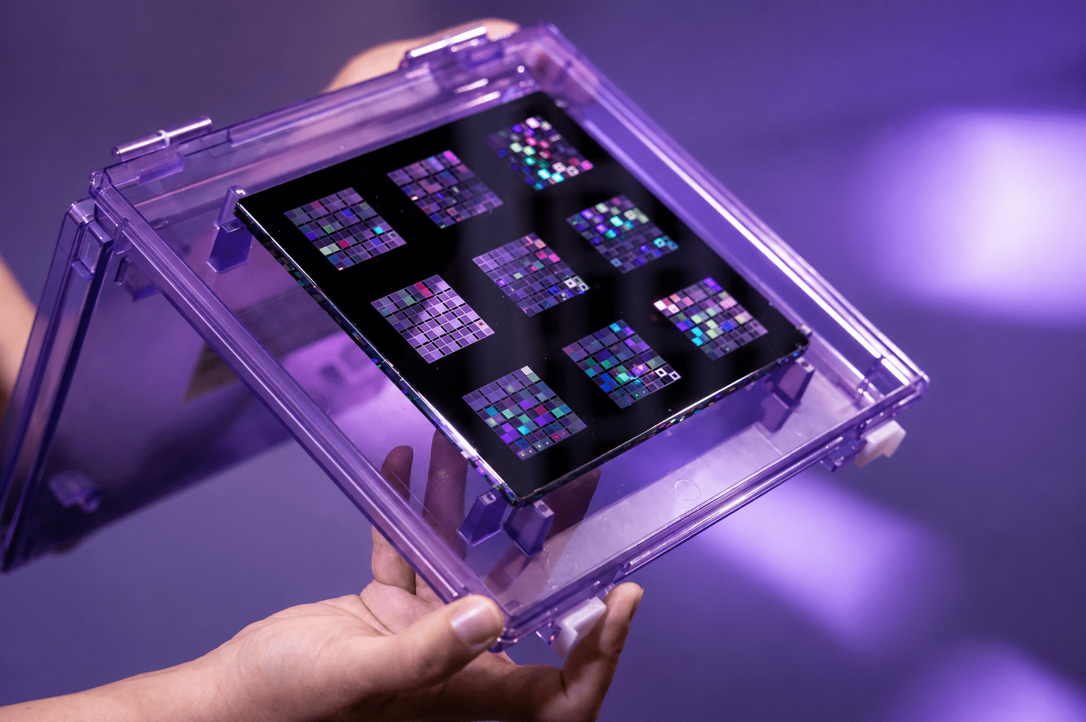
Mask & Resist Technology. For maximum resolution and process efficiency.
Chip-Services. Für Forschung und Entwicklung.
For more than 15 years, IMS CHIPS has operated an in-house mask line for binary and phase-shift masks in 6025 and 9035 formats. In parallel, we evaluate and develop electron-beam resists for high-resolution patterning while maintaining practical processing throughput.
Our resist development also includes combinations with conductive layers designed to minimize charging effects during electron-beam lithography.

Reference projects in nanostructuring.
Technologies that make a difference.
Nanopatterning requirements vary widely depending on the application, substrate, feature size, and fabrication process. The following projects illustrate how IMS CHIPS combines process development and high-precision manufacturing to address specific challenges in research and industrial applications.
Extremely Large Telescope (ELT)
High-precision optics require exceptional control over both feature geometry and reproducibility. For the Extremely Large Telescope (ELT) of the European Southern Observatory (ESO), IMS CHIPS manufactured diffractive optical elements used in the metrology and fabrication of segments for the telescope’s 39-meter primary mirror (M1).
The project demonstrates our capabilities in developing and manufacturing high-precision optical nanostructures for applications with demanding accuracy and reproducibility requirements.
Nanoimprint master. From single pieces to high-precision replication.
In collaboration with EV Group, IMS CHIPS developed and manufactured a high-precision nanoimprint master featuring a color miniature of the Stuttgarter Schloss (palace). Rather than relying on pigments, the vivid colors are generated entirely by diffractive nanostructures engineered to interact with light.
IMS CHIPS manufactured the master, while EVG used nanoimprint technology to replicate the pattern. The project demonstrates how precisely engineered nanostructures can create optical functionality and opens up opportunities for functional surfaces and security-related applications.