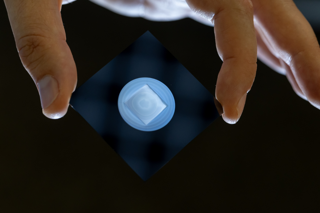
Get started now.

“Every MEMS project starts with understanding what the application needs to achieve. Together, we define the required functionality, materials, dimensions, geometry, and level of integration. From there, we develop the appropriate process flow, evaluate feasibility, fabricate prototypes, and refine the design toward a robust, scalable solution. If you have a MEMS challenge in mind, I’d be happy to discuss it with you.”
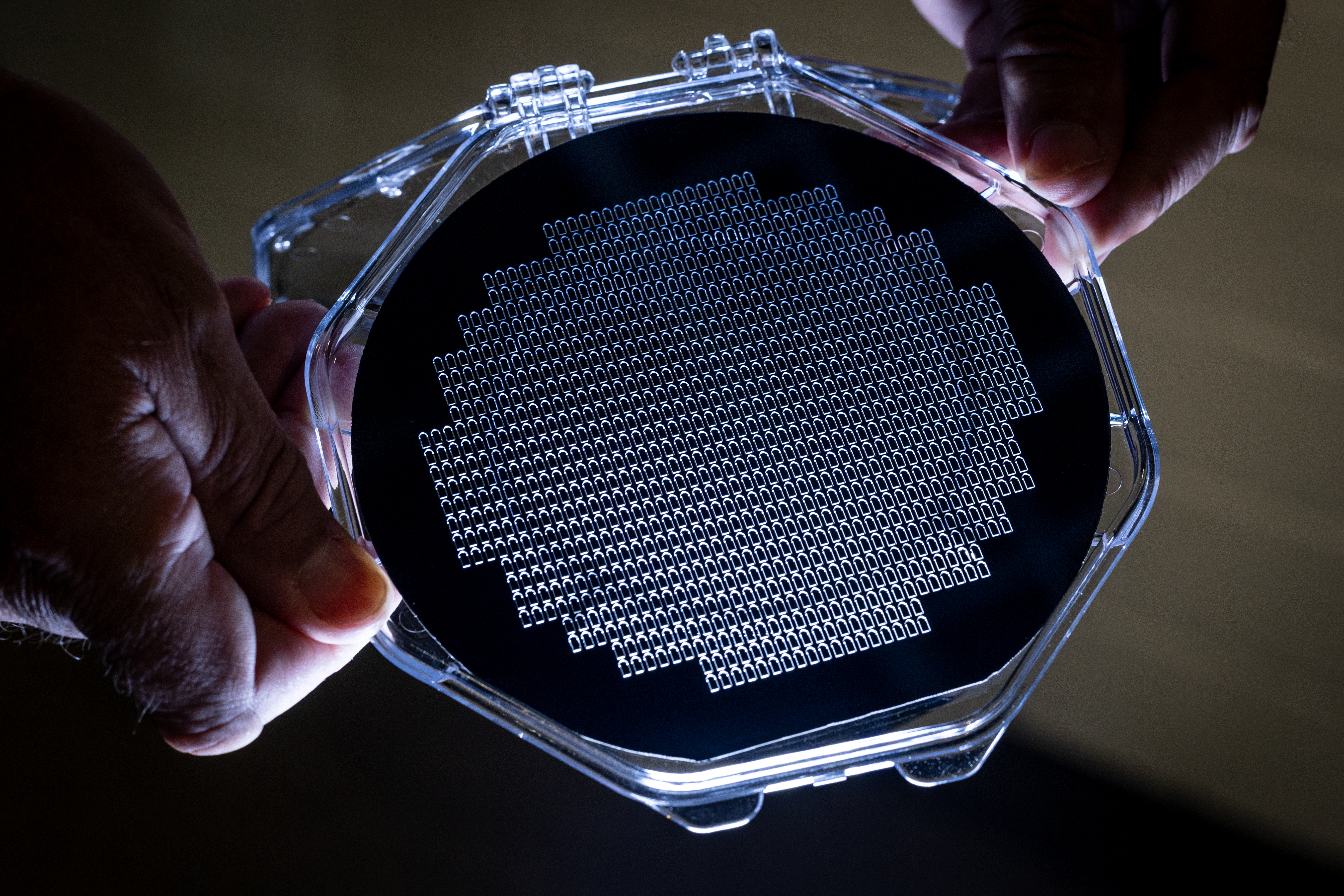
Membranes. Individually-designed for your application.
We fabricate membranes in a range of geometries, dimensions, and materials to match the requirements of the application. Structures can be patterned directly into the membrane to create stencil masks or, for Si₃N₄ membranes, into thin chromium absorber layers to produce absorber masks. The result is a membrane solution engineered for applications in optics, sensing, and energy systems.
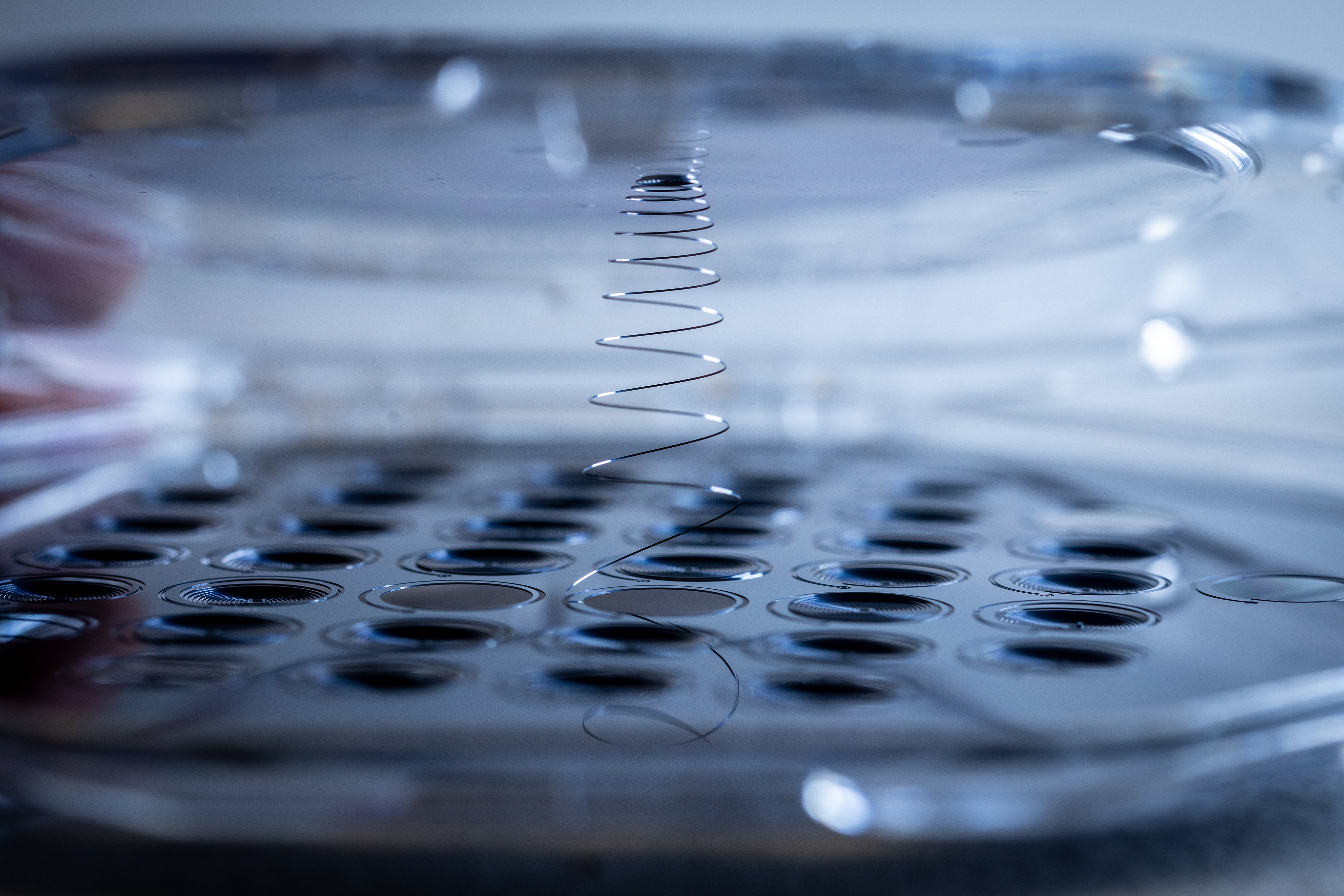
Micromechanics. For complex silicon structures with feature sizes up to 50 nm.
THE IMS CHIPS SOI wafer process and the two in-house variable-shaped electron-beam writers enable silicon structures with feature sizes down to 50 nm in membranes only a few hundred nanometers thick. For larger-scale structures, our in-house stepper, laser, and contact lithography capabilities provide a cost-effective alternative, including structures etched through the entire wafer substrate.
This combination gives developers access to fabrication technologies spanning nanoscale features and macroscopic silicon structures within a single technology portfolio.
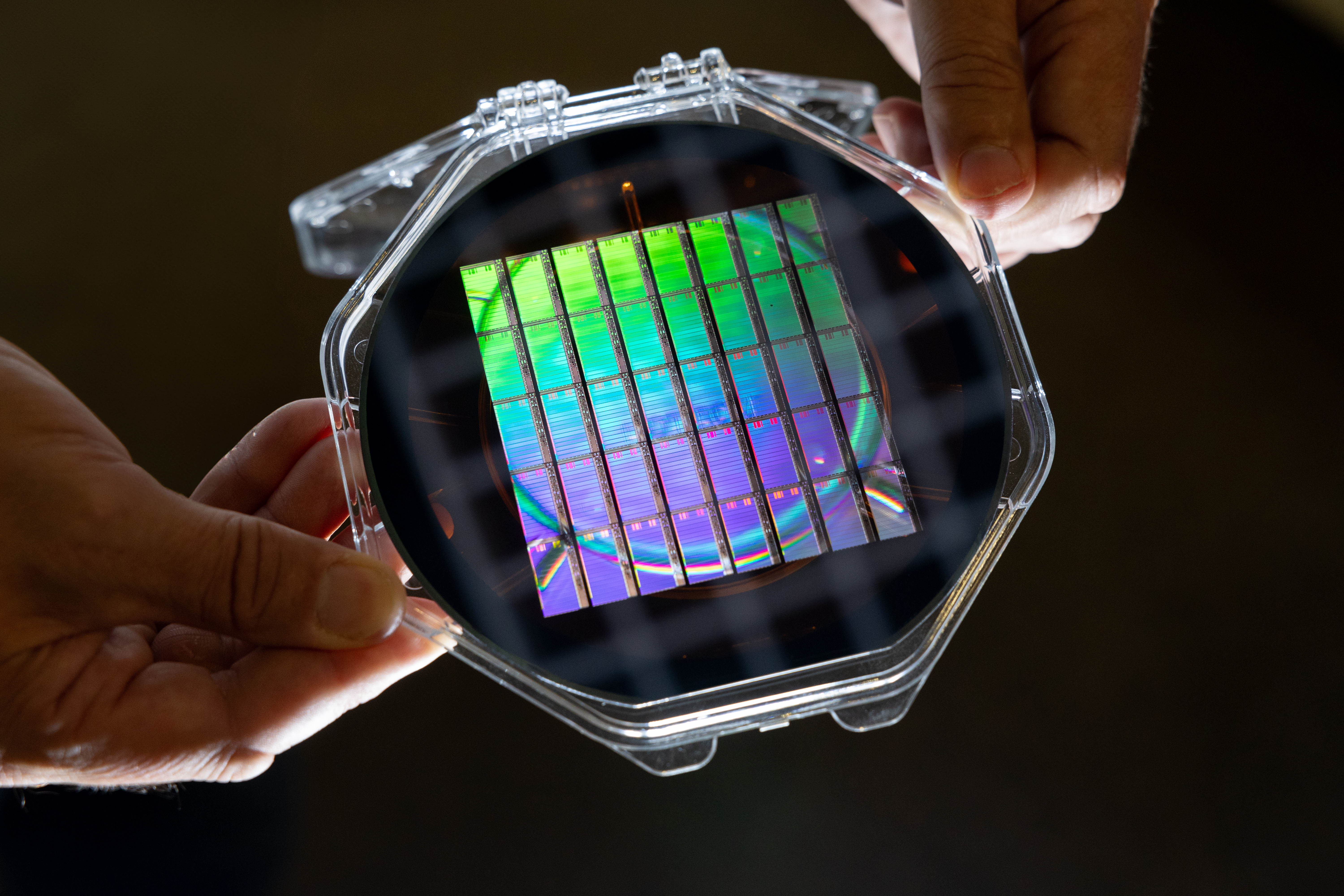
CMOS post-processing. MEMS integration directly onto finished CMOS chips.
Fully processed CMOS wafers can be further modified at IMS CHIPS through deep silicon etching, selective thinning, layer deposition, and additional patterning. These processes are available for both foundry wafers and substrates processed in-house.
Precise alignment enables CMOS circuitry and micromechanical components to be integrated and electrically interconnected. Our assembly, adhesive bonding, and chip-bonding capabilities also make it possible to combine multiple active and passive dies into complex chip stacks with sub-micrometer alignment accuracy. This provides a flexible route to highly integrated microsystems for a broad range of applications.